المنتجات الساخنة
PCB Fabrication Process Flow Chart pcbelec
2022-2-7 PCB, or printed circuit board, is an important electronic part and the support body of electronic components. Because it is made by electronic printing, it is called “printed” circuit board. Electronic products in the production process, there will be a
Contact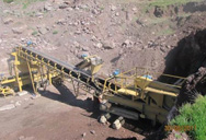
A flow chart to understand PCB designing process
2015-12-17 PCB design flow chart explains various steps involved in the process of PCB designing. QualiEco Circuits Limited has the potential to be an excellent supplier to us! that we receive from QualiEco Circuits. Always deliver what is
Contact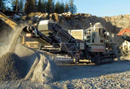
Flow-chart of a printed circuit board production (PCB)
2014-11-7 Flow-chart of a printed circuit board production (PCB) not necessary for simple single-side PCBs, because the photo resist is applied negative and serves as etch resist photo resist apply, expose, develop stacking of panels drilling scrubbing apply etch resist strip photo resist etch strip etch resist check solder solder mask:
Contact
PCB Layout Design Flowchart mtipcb
2015-12-10 PCB Layout Design Flowchart mtipcb COMPANY DRAWINGS TEMPLATE BOARD OUTLINE DRAWING Microtrack Printed Circuit Design PCB Layout Services Since 1982 Office: 802-877-3167 Cell: 802-238-5641 Quotes: mtipcb E-mail: design@mtipcb MAP GROUPS TO BOARD AREA Arrange circuit blocks on board per
Contact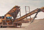
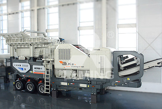
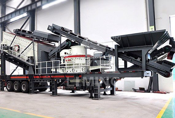
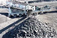
PCB Shredder / PCB Crusher / Printed Circuit Board Shredder
PCB Shredder / PCB Crusher / Printed Circuit Board Shredder. Printed circuit board is also known as PCB or green board. They are used to mechanically support and electrically connect electronic components using conductive pathways, traces, etched from copper sheets laminated onto a non-conductive substrate.
Contact
Recycling of Printed Circuit Boards IntechOpen
2018-9-25 Recycling of Printed Circuit Boards 287 beryllium in the electronics industry is as beryllium oxide which transmits heat very efficiently and is used in heat sinks. Typically PCBs contain about 5%weight of Fe, 27% of Cu, 2% of Al and 0.5% of Ni, 2000 ppm of Ag 80 ppm of Au; however there is no average scrap composition and the values
Contact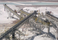
Printed circuit boards manufacturing karadev.net
2017-7-30 Printed circuit boards manufacturing virtually every circuit board uses this material, although there will be differences in the final surface finish. The board consists of resin, reinforcement, copper foil, and of course a lamination process. 2 There is a finite period of time during which the resin remains fluid enough to flow freely
Contact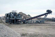
How to Build a Printed Circuit Board 4pcb
2014-11-12 How to Build a Printed Circuit Board. Advanced Circuits Inc 2004 2 This presentation is a work in progress. As methods and processes change it will be updated accordingly. It is intended only as an introduction to the production processes used in building a circuit board and as a training aid for employees, customers and friends of Advanced
Contact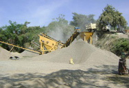
Crushing performance and resource characteristic of
The crushing performance of printed circuit board (PCB) was studied on several crushers. The results show that PCB is a material which is difficult to crush.
Contact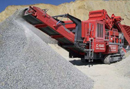
IPC-1601A: Printed Board Handling and Storage
2020-10-13 Printed Board Handling and Storage Guidelines 1 INTRODUCTION 1.1 Background Historically, the printed board industry has relied on military specifications and guidelines to define packaging methods to preserve the quality and reliability of printed boards during shipment and storage.
Contact
A method for quality improvement of waste printed circuit
2021-2-20 The flow chart of this study is shown in Fig. 2.FS200 universal crusher was selected to obtain the crushing WPCBs, and the features of this crusher has been described in our former research (Yan et al., 2020).The adjusted parameters are feed volume ratio and crushing time.
Contact
Selectivity crushing of discarded printed circuit boards
Taking printed circuit board(PCB) with highly enriched metal size ranging from 0.125 mm to 0.5 mm as materials for separation, the influence of air flow rate on the separation efficiency of high
Contact
PCB Shredder / PCB Crusher / Printed Circuit Board Shredder
PCB Shredder / PCB Crusher / Printed Circuit Board Shredder. Printed circuit board is also known as PCB or green board. They are used to mechanically support and electrically connect electronic components using conductive pathways, traces, etched from copper sheets laminated onto a non-conductive substrate.
Contact
Recycling of Printed Circuit Boards IntechOpen
2018-9-25 Recycling of Printed Circuit Boards 287 beryllium in the electronics industry is as beryllium oxide which transmits heat very efficiently and is used in heat sinks. Typically PCBs contain about 5%weight of Fe, 27% of Cu, 2% of Al and 0.5% of Ni, 2000 ppm of Ag 80 ppm of Au; however there is no average scrap composition and the values
Contact
CHAPTER 12: PRINTED CIRCUIT BOARD (PCB) DESIGN
2019-5-10 CHAPTER 12: PRINTED CIRCUIT BOARD (PCB) DESIGN ISSUES Introduction Printed circuit boards (PCBs) are by far the most common method of assembling modern electronic circuits. Comprised of a sandwich of one or more insulating layers and one or more copper layers which contain the signal traces and the powers and grounds, the
Contact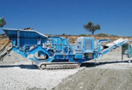
Signal Integrity for High-Speed Design in PCB Layout
2022-1-20 Signal integrity basics in printed circuit boards. Layout recommendations for combating signal integrity problems in PCB designs. PCB layout features, functions, and tools that will help you with good signal integrity in your design. (PDN) should have wide traces and vias to increase the flow of current and reduce the amount of inductance.
Contact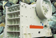
Printed Circuit Boards Assembly (PCBA) Process PCBCart
An advanced circuit board won't be able to give its functionality until components are mounted on it. A PCB with components mounted on is called an assembled PCB and the manufacturing process is called PCB assembly or PCBA for short. The copper lines on bare board, called traces, electrically link connectors and components to each other.
Contact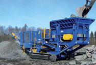
Pyrolysis of Printed Circuit Boards SMTnet
2013-10-3 Pyrolysis of Printed Circuit Boards T. R. Mankhand *, K. K. Singh, Sumit Kumar Gupta, Somnath Das Department of Metallurgical Engineering, Indian Institute of Technology (Banaras Hindu University),Varanasi, 221005, India Abstract Printed Circuit Board (PCB) is an essential component of almost all electrical and electronic equipments. The
Contact
IPC-1601A: Printed Board Handling and Storage
2020-10-13 Printed Board Handling and Storage Guidelines 1 INTRODUCTION 1.1 Background Historically, the printed board industry has relied on military specifications and guidelines to define packaging methods to preserve the quality and reliability of printed boards during shipment and storage.
Contact
How to Make a Printed Circuit Board (PCB) PCB Maker Pro
2018-3-20 A printed circuit board has pre-designed copper tracks on a conducting sheet. The pre-defined tracks reduce the wiring, thereby reducing the faults arising due to loose connections. One simply needs to place the components on the PCB and solder them. In this tutorial, I will show you how you can make circuit boards at home easily.
Contact
printed circuit board process flow chart Leappcb
2020-2-20 联系我们 CONTACT US 联系人:曾小姐 手机:008613928048496 电话:0755-28628518 邮箱:leappcb@163,sales@leappcb 地址: 中国广东省深圳市宝安沙井洪田
Contact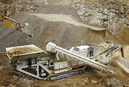
printed circuit board process flow chart Leappcb
Smart products expand FPC soft board market space 2019-06-29 What-should-I-do-if-the-crystal-on-the-board-is-broken 2019-06-01 Component placement order on the PCB 2019-03-05
Contact
A method for quality improvement of waste printed circuit
2021-2-20 The flow chart of this study is shown in Fig. 2.FS200 universal crusher was selected to obtain the crushing WPCBs, and the features of this crusher has been described in our former research (Yan et al., 2020).The adjusted parameters are feed volume ratio and crushing time.
Contact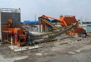
Printed Circuit Board Process Flow Orient Display
2022-2-7 The Printed Circuit Board (PCB) manufacturing process can be summarized as the following steps: 1. Cutting. Cutting is the process of cutting the dry-cleaned copper-clad panel into small pieces according to the production size, which can be fabricated on the production line. To ensure safe operation and reduce scratch issues, the corners of the
Contact
PCB Shredder / PCB Crusher / Printed Circuit Board Shredder
PCB Shredder / PCB Crusher / Printed Circuit Board Shredder. Printed circuit board is also known as PCB or green board. They are used to mechanically support and electrically connect electronic components using conductive pathways, traces, etched from copper sheets laminated onto a non-conductive substrate.
Contact
Recycling of Printed Circuit Boards IntechOpen
2018-9-25 Recycling of Printed Circuit Boards 287 beryllium in the electronics industry is as beryllium oxide which transmits heat very efficiently and is used in heat sinks. Typically PCBs contain about 5%weight of Fe, 27% of Cu, 2% of Al and 0.5% of Ni, 2000 ppm of Ag 80 ppm of Au; however there is no average scrap composition and the values
Contact
CHAPTER 12: PRINTED CIRCUIT BOARD (PCB) DESIGN
2019-5-10 CHAPTER 12: PRINTED CIRCUIT BOARD (PCB) DESIGN ISSUES Introduction Printed circuit boards (PCBs) are by far the most common method of assembling modern electronic circuits. Comprised of a sandwich of one or more insulating layers and one or more copper layers which contain the signal traces and the powers and grounds, the
Contact
IPC-1601A: Printed Board Handling and Storage
2020-10-13 Printed Board Handling and Storage Guidelines 1 INTRODUCTION 1.1 Background Historically, the printed board industry has relied on military specifications and guidelines to define packaging methods to preserve the quality and reliability of printed boards during shipment and storage.
Contact
Pyrolysis of Printed Circuit Boards SMTnet
2013-10-3 Pyrolysis of Printed Circuit Boards T. R. Mankhand *, K. K. Singh, Sumit Kumar Gupta, Somnath Das Department of Metallurgical Engineering, Indian Institute of Technology (Banaras Hindu University),Varanasi, 221005, India Abstract Printed Circuit Board (PCB) is an essential component of almost all electrical and electronic equipments. The
Contact
FPC (Flexible Printed Circuit): The Manufacturing Process
2019-1-14 FPC is a thin insulating polymer film that conductive circuit patterns are printed on and typically it’s supplied with a thin polymer coating to protect the circuit. The material and the structure grant the FPC flexibility, which allow it to
Contact